
I. Background and Application Needs
In the fields of cell engineering, biomaterials, and drug delivery systems, high-throughput microstructured chip platforms are becoming a key research tool. Especially platforms combining PDMS micropillar array chips with controlled biodegradable thin films (e.g., PLGA) are widely used in:
- Single-cell drug delivery and sensitivity evaluation;
- Cell-material interface interaction studies (adhesion, migration, differentiation);
- Multi-factor high-throughput screening and biomimetic microenvironment construction;
- Precise control of nanoscale drug release behavior.
These applications often require construction of highly uniform, nanometer-scale (100–300 nm) functional film layers specifically on the tops of the pillars, with PLGA (poly(lactic-co-glycolic acid)) as the typical material due to its biocompatibility, biodegradability, and tunable release properties.
However, traditional planar spin coaters with vacuum suction platforms are not suitable for achieving uniform nanoscale coatings on non-planar structures like micropillars, especially when coating only the pillar tops. This presents a demand for a specially designed spin coater to meet these challenges.
II. Spin Coating Principle Overview
Spin coating is a widely used technique in microelectronics, optics, and biomaterials for the rapid formation of uniform thin films. The basic steps include:
- Dropping solution onto a substrate;
- Rapid rotation creates centrifugal force spreading the liquid evenly;
- Simultaneous solvent evaporation leads to film formation within seconds.
Based on simplified Meyerhofer’s model, film thickness “h” relates to:
h ∝ (c * μ) / ω^{1/2}
Where:
- c = solution concentration;
- μ = viscosity;
- ω = rotation speed (rpm);
By adjusting these parameters, film thicknesses from tens to hundreds of nanometers can be reliably achieved. For pillar-top coating, this must be combined with specialized jigs, non-vacuum mechanisms, and multi-stage programmatic rotation control.
III. Functional Requirements for the Spin Coater
To satisfy the target application, the spin coater must meet the following specifications:
1. Microstructure-Compatible Platform
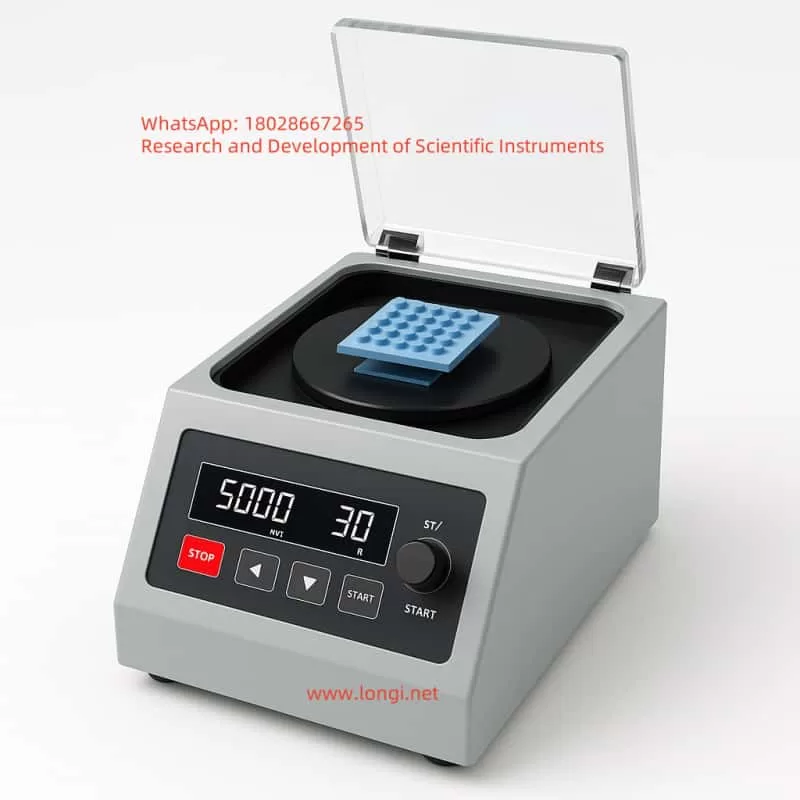
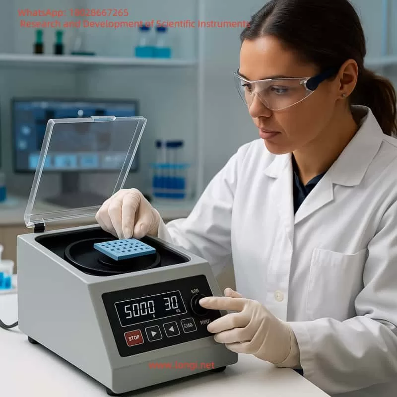
- Substrate size: 55 mm × 55 mm PDMS chip;
- Non-vacuum clamping to prevent microstructure collapse;
- Compatible with curved/non-planar substrates for optimal pillar-top coating.
2. Precision Rotational Control
- Speed range: 100–10,000 rpm;
- Speed resolution: 1 rpm;
- Acceleration range: 100–10,000 rpm/s;
- Multi-stage programmable control (min. 10 segments);
- Each stage must set: speed, time, acceleration.
3. Nanofilm Thickness Control Module
- Automated dispensing system (micro syringe pump):
- Volume range: 0.1–10 μL;
- Precision: ±0.01 μL;
- Optional heating lid (to improve uniform solvent evaporation);
- Environmental sealing (for use inside glovebox);
- Gas inlet for nitrogen or controlled airflow.
4. Software and Feedback Control
- Color LCD touchscreen for programming and monitoring;
- Real-time display of speed, time, temp, steps;
- At least 20 custom program sets storage;
- USB export of spin data logs;
- External sensor interfaces (e.g., ellipsometer, IR monitor).
IV. Key Innovation Highlights
- Non-vacuum clamping system:
- Avoids PDMS micropillar collapse;
- PTFE precision slot clamp secures the chip without central blockage.
- Pillar-top coating optimization:
- Multi-stage program: pre-spread (low speed), main spin (high speed), dry-out (moderate speed);
- Sample protocol: 300 rpm (10s) → 2000 rpm (30s) → 1000 rpm (20s).
- Micro-volume drop dispensing system:
- Controlled center-drop of PLGA solution (2–5 wt% in DCM);
- Precision stage and optional laser alignment.
- Anti-edge-thickening logic:
- Delay spin or pre-wet stage to prevent solution migrating to chip edges.
- Open programming interface:
- Supports MATLAB / Python SDK;
- Integration with AI or bioassay automation platforms.
V. Workflow Example
- Deposit 0.5–2 μL PLGA solution at the center of PDMS chip;
- Spin program:
- Step 1: 300 rpm for 10 s (pre-spread);
- Step 2: 2000 rpm for 30 s (uniform coating);
- Step 3: 1000 rpm for 20 s (controlled dry);
- Optional: N2 gas flow to assist solvent removal;
- Post-process: film thickness validated by ellipsometry or AFM.
VI. Implementation and Materials
- Control system: STM32/ESP32 + encoder + BLDC driver;
- Syringe pump: stepper-driven microinjection with replaceable tips;
- Heating lid: PTFE shell + PTC film heater + PID temp control;
- Housing: CNC-machined aluminum frame + acrylic protective cover;
- Chip holder: laser-cut PTFE tray, supporting 3–4 mm thick PDMS chips.
VII. Market Benchmarks and Outlook
Comparison with existing devices:
- Ossila Advanced Spin Coater (UK);
- Laurell WS-650 series (USA);
- MTI VTC-100PA (China);
Our design focuses on the niche need for micropillar-top nanofilm coating in biological applications, filling a gap in existing commercial equipment that primarily supports flat wafer processing.
Future development roadmap includes:
- Multi-solution switching module (e.g., for combinatorial screening);
- Vision-assisted chip alignment and coating path planning;
- Closed-loop AI control based on film thickness feedback.
VIII. Conclusion
This design addresses the unmet need for high-precision nanocoating on micropillar arrays in PDMS chips—especially relevant in single-cell drug screening and cell-material interface studies. By integrating multi-stage programmable spin control, non-vacuum platform, microfluidic injection, and programmable environment conditioning, this spin coater provides a complete solution for researchers working on nanoscale PLGA film deposition in structured biological interfaces.
It is expected to contribute significantly to advanced biomedical research, high-throughput drug screening, and future bioMEMS development.